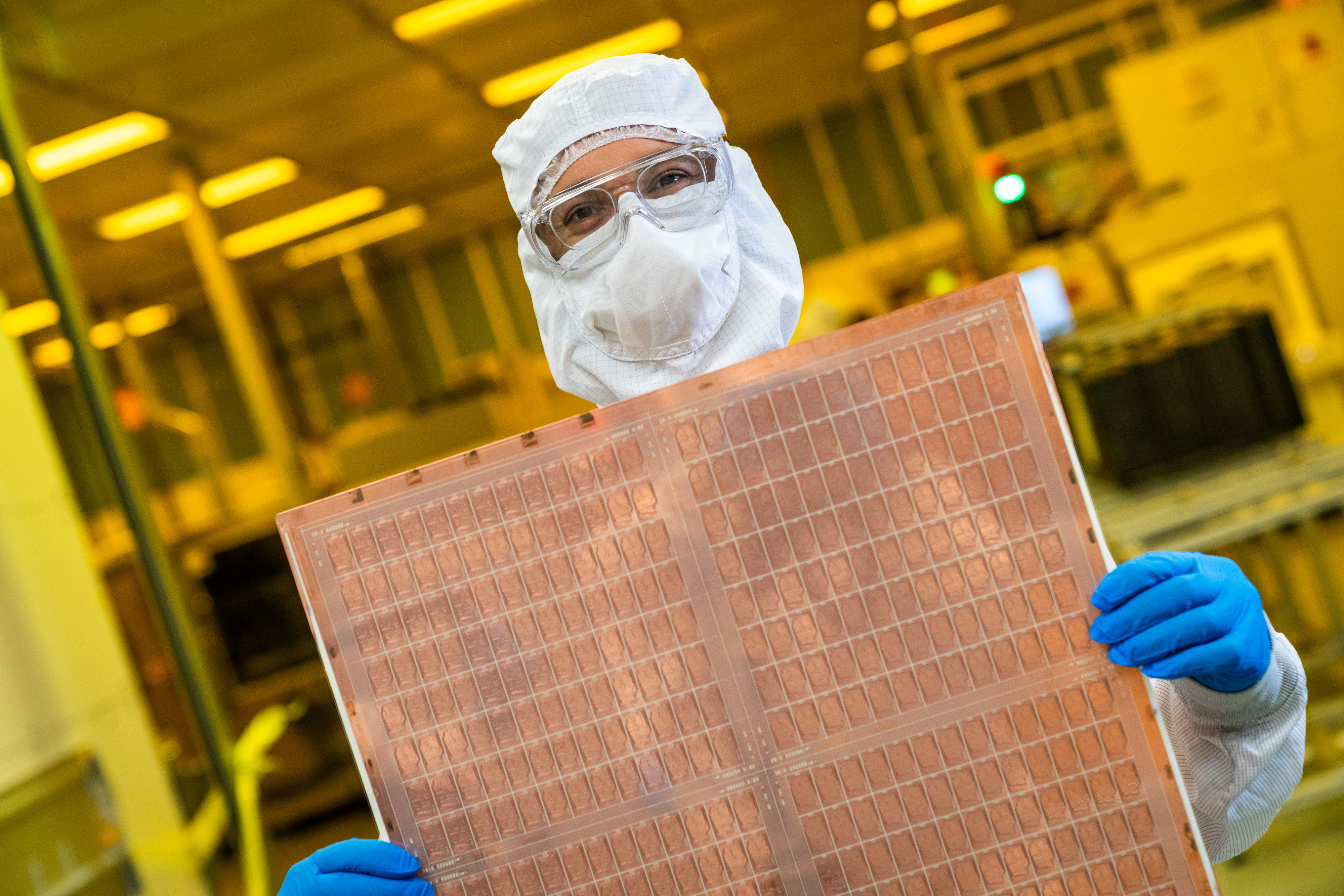
ASE Technology is committing $200 million to test a new method of chip packaging that replaces traditional round wafers with square substrates, which promises to increase the company's advanced packaging output, reports Nikkei. For now, the company plans to set up a rather small-scale trial production line, but the rather large sum that ASE plans to invest indicates that it is serious about using next-gen substrates.
ASE plans to set up a test production line in Kaohsiung, Taiwan, where it would install experimental machines that will process 600mm × 600mm substrates instead of 300-mm round wafers. As no ready-to-use machines can process such large square substrates that meet the requirements of semiconductor-grade production, ASE is collaborating with suppliers to develop the tools to make this technology feasible.