
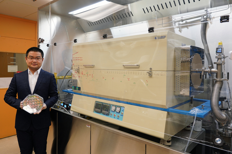
The increasing need for more powerful, faster, and more efficient computing capabilities has been met with increasingly difficult materials and engineering problems as attempts at performance scaling continue. As published on Nature, MIT engineers have developed a new silicon fabrication process that works by depositing three-atom thick, atomically thin transistors (ATTs) on top of already-existing chip circuits – essentially “growing” them into high-density, high-performance computing stacks.
The team’s novel approach looks something like additive manufacturing, and applies a highly uniform, three-atom-thick layer of 2D Transition Metal Dichalcogenide (TMD) materials across an entire 8-inch, fully fabricated silicon wafer. Each new layer of TMD enables denser integrations between the underlying chip and the added transistor stacks, improving performance with unparalleled density.